At NEOTech, we lead the way in Ceramic Substrate manufacturing, offering unmatched expertise and quality in the production of Low Temperature Co-fired Ceramic (LTCC), High Temperature Co-fired Ceramic (HTCC) packages, and Thick Film substrates.
Our comprehensive services support applications across a variety of markets, including Aerospace & Defense, Medical, and High-Tech Industrial sectors, where robust, high-performance substrates are essential.
NEOTech’s ceramic substrate capabilities cover a range of advanced materials and designs ideal for stable performance in both cryogenic and high-temperature environments. Our offerings include:
We are recognized globally as a leader in multilayer ceramic manufacturing, delivering reliable substrates for applications in sectors that demand top-tier quality and performance.
Our ceramic substrates are essential to a range of high-reliability applications, such as:
At NEOTech, quality management is embedded in everything we do. Our ceramic substrate manufacturing facility operates with a full suite of certifications and rigorous risk management protocols, including:
Our continuous improvement initiatives and cost-reduction programs are designed to enhance efficiency while ensuring the highest level of quality and reliability for our customers.

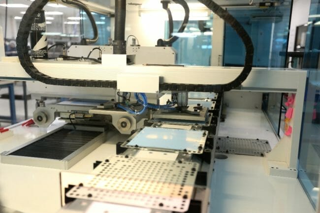
NEOTech provides a variety of engineering services directly at our ceramic substrate facility, offering our customers a streamlined build-to-print experience with co-located engineering support. Services include:
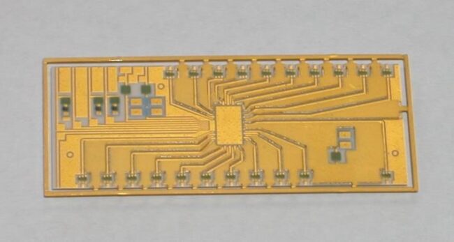
Our in-house capabilities for fabricating HTCC and LTCC ceramic substrates allow us to maintain strict controls and offer substrates with hermetic sealing, multilayer capabilities up to 50+ layers, and superior thermal performance. We also offer thick film technology, BeO substrates, and additional substrate finishing processes like plating and etch-back.
NEOTech’s LTCC and AIN solutions deliver high-interconnect density, compactness, and performance for high-frequency applications. Benefits include:
As a trusted partner to leading defense, space, and high-reliability electronics OEMs, NEOTech brings unparalleled experience and dedication to ceramic substrate manufacturing. Our team of engineers and technicians is committed to delivering the highest quality products that meet the exacting standards of our customers.
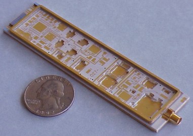
Low Temperature Co-fired Ceramic (LTCC) is a multi-layer ceramic PCB solution that provides high frequency performance with gold and silver conductors. LTCC substrates offer additional functionalities, serving as smart substrates, structural components, and multi-purpose packages.
High Temperature Co-fired Ceramic (HTCC) provides the highest level of hermetic sealing and strength, ideal for high-reliability applications such as defense electronics, infrared sensors, and aerospace systems. NEOTech offers both Aluminum Nitride and Alumina HTCC, each delivering superior thermal conductivity and protection in challenging environments.
Plating Options
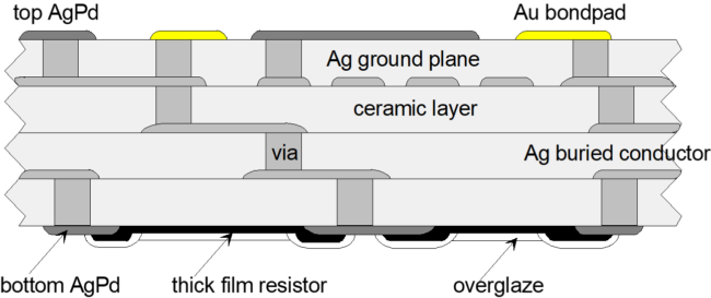
Thick Film Systems
NEOTech offers standard Thick Film Substrates used in most signal and low power applications. We work with a variety of substrates including BeO, AlN and Alumina (Al2O3).

LTCC and HTCC technology is a unique solution for high-interconnect density and compact networks, as well as high frequency applications. Key advantages include:
Ceramic Substrate manufacturing includes:
Ceramic Substrate manufacturing includes:
NEOTech also provides next generation Etch Conductor Photolithography (ECP) Thick Film Substrates suitable for microwave and high-resolution lines and space applications. The Thick Film conductor material is fired in a dense, non-porous film over a large area of the substrate. The high resolution lines are then defined using photoresist and etch techniques to achieve widths and spaces as low as 0.003″ (0.0762mm). The ECP process is based around standard thick film Au that is already qualified by many OEMs, thus avoiding long qualification cycles and bringing customers to market quickly. ECP technology allows designers to combine RF and digital functions on substrates, and offers options for integrating capacitors, resistors, inductors, couplers, and filters. Capacitors and resistors can be laser trimmed to obtain +/-3% and +/-1% tolerances, respectively.
With more than forty years of expertise in high-reliability hybrid and RF technologies, NEOTech has established itself as the largest provider of microelectronics assembly services in North America. We offer a comprehensive array of services encompassing the design, development, and manufacturing of microelectronic assemblies, specializing in microwave electronics and circuits. Our dedicated teams are committed to delivering technical support and advanced testing for microelectronic assemblies, ensuring superior quality and reliability for our customers.
Offshore manufacturing strategies are collapsing under the weight of rising tariffs, unpredictable logistics, and quality control challenges. NEOTech offers a smarter path forward—with trusted U.S. and Mexico-based electronics manufacturing services built for resilience, agility, and excellence.